14-Layer High Density Interconnect (HDI) PCB Built on FR-4 Tg170℃ with Immersion Gold
(Custom PCBs are tailored products; the images and specifications provided are for reference only.)
General Description
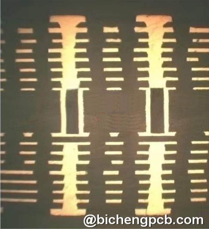
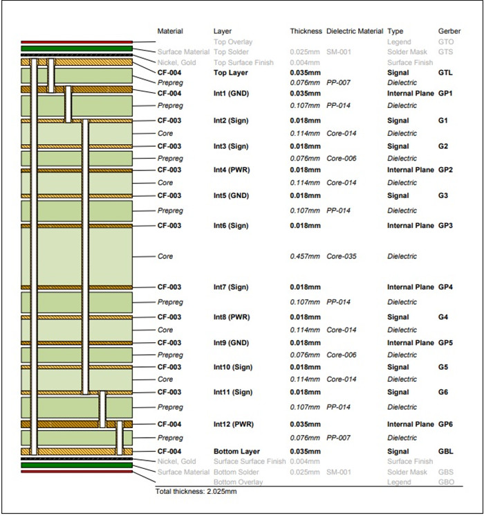
This 14-layer HDI printed circuit board is constructed on an FR-4 Tg170 substrate, designed for codec equipment applications. It has a thickness of 2.0 mm, features a white silkscreen on a green solder mask, and utilizes immersion gold on the pads. The PCB includes high-density interconnection layers with blind vias connecting L1-L2, L13-L14, and buried vias connecting L3-L4, L4-L12, and L12-L13. Microvias are stacked across different layers. The base material is sourced from ITEQ, with one board per panel. The PCBs are manufactured according to IPC 6012 Class 2 standards using the provided Gerber data, with each shipment containing 20 panels.
Our Advantages
1.ISO9001, ISO14001, IATF16949, UL Certified
2.Prototype to volume production capabilityB
3.16,000㎡ workshop
4.30,000㎡ output capacity per month
5.8,000 types of PCBs produced monthly
6.IPC Class 2 / IPC Class 3 compliance
7.First production eligible products rate: >95%
Applications of HDI PCBs
Automotive
GPS Trackers
5G WiFi
Embedded Systems
Smartphones and Tablets
Wearable Technology and Healthcare
Access Control Solutions
Aerospace
.jpg)
Parameter and Data Sheet
| Number of Layers | 14-Layer |
| Board Type | Multilayer PCB |
| Board size | 220mm x 170mm=4PCS |
| Board Thickness | 2.0 mm +/-0.16 |
| Board Material | FR-4 |
| Board Material Supplier | ITEQ |
| Tg Value of Board Material | 170℃ |
| PTH Cu thickness | ≥20 um |
| Inner Iayer Cu thicknes | 18 um (0.5oz) |
| Surface Cu thickness | 35 um (1oz) |
| Solder Mask Type and Model No. | LPSM, PSR-2000GT600D |
| Solder Mask Supplier | TAIYO |
| Solder Mask Colour | Green |
| Number of Solder Masks | 2 |
| Thickness of Solder Mask | 14 um |
| Type of Silkscreen Ink | IJR-4000 MW300 |
| Supplier of Silkscreen | TAIYO |
| Color of Silkscreen | White |
| Number of Silkscreen | 1 |
| Mininum Trace (mil) | 5.8 mil |
| Minimum Gap(mil) | 6.2 mil |
| Surface Finish | Immersion Gold |
| RoHS Required | Yes |
| Warpage | 0.25% |
| Vias | Blind vias L1-L2, L13-L14, buried vias L3-L4, L4-L12, and L12-L13, Through holes. |
| Thermal Shock Test | Pass, 288±5℃,10 seconds, 3 cycles. No delamination, no blistering. |
| Solderablity Test | Pass, 255±5℃,5 seconds Wetting Area Least 95% |
| Function | 100% Pass electrical test |
| Workmanship | Compliance with IPC-A-600H & IPC-6012C Class 2 |
Different Types of HDI PCBs
To simplify the classification of high-density interconnect PCBs, we define three types of HDI PCBs as follows:
1+N+1: PCBs that contain one-time laser drilling and pressing.
I+N+I (I≥2): PCBs that include two or more laser drilling and pressing steps, featuring staggered or stacked microvias across different layers.
Any Layer HDI: Blind and buried vias can be placed freely on various layers as per the designer's requirements.